| Home | Research | People | Publications | Teaching | Opening | News | Contact |
|
Enabling Technologies
|
|||
This research is centered around developing a fundamental understanding of the physical processes underlying intense ultrafast laser-interaction with materials, with applications ranging from materials processing to spectroscopic analysis. The basic processes of intense ultrafast laser-material interaction can be categorized into three stages that cover a time span of 109 s, from femtoseconds to microseconds: Electronic Excitation and Relaxation (1 fs – 1 ps); Molecular Motion and Plasma Initiation (100 fs – 1 ns); and Hydrodynamic Plasma Development (100 ps – 1 ms). While a significant body of research has been focused on intense ultrafast laser-induced electronic excitation as well as hydrodynamic expansion of a fully-developed laser plasma, there has been little understanding of how plasma is initiated. We are developing a comprehensive theoretical model to describe femtosecond laser-induced plasma initiation process, and conducting experiments to examine the characteristics of the plasma in its formation stage.
[1] S. S. Mao, F. Quéré, S. Guizard, X. Mao, R. E. Russo, G. Petite, and P. Martin, “Dynamics of femtosecond laser interactions with dielectrics.” Applied Physics A, V.79, 1695 (2004). [Invited/Review]
|
 |
||
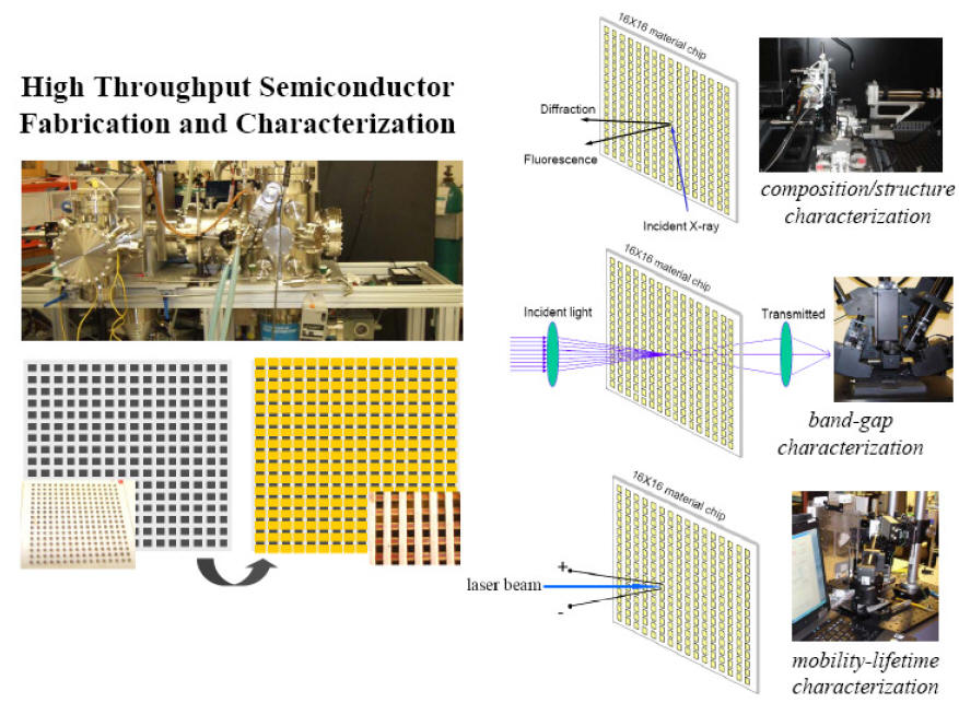
Conventional approaches for semiconductor material growth typically involve fabricating one sample at a time, either in the form of a bulk single crystal or a thin film. In contrast, a combinatorial thin film approach that employs a suite of area-selecting masks to delineate regions with different composition allows hundreds of samples to be fabricated in one growth cycle. This parallel material fabricating technique can help discover new semiconductors for applications ranging from photovoltaic solar cells to radiation detectors. We have established a combinatorial semiconductor thin film growth facility, and developed high throughput semiconductor characterization techniques for measuring the composition, structure, optical, and transport properties of the combinatorial thin film libraries. We are applying this unique high throughput material screening facility to develop high performance semiconductors for better solar cells and detectors.
[1] S. S. Mao, “High throughput combinatorial screening of semiconductor materials.” Applied Physics A, V.105, 283 (2011). [Invited/Review]
|
|
||
| University of California at Berkeley |
this page is under construction |
||